MCB's (Not PCB's)

Brent Dowell

Administrator
Staff member
Messages
16,600
Location
Reno NV
A while back I had bought a little desktop 3018 cnc machine with the thoughts I could use it to make circuit boards. Not really PCB's, but MCB's (Milled Circuit Boards).

Been playing with it for a while and it's been a bit of a learning curve to get through, but I've finally got it down I think.

I was wanting to update the shelves I use for my Record collection. I had put some addressable led strips on them before, but did not like the way I had the leds strips mounted. I had them on some brackets that held them out in front. I ordered some new shelves (as I needed more room). They are the standard ikea type crap, but they should work to hold records till I get tired of them and someday make something else to hold them. At any rate, I 'modified' the shelves to add a dado in them to hold the light strips. Thats the only part of this project that is remotely woodworking related.

There is a library out there called "WLED" that works with addressable led strips/strings that runs on ESP32 microcontroller boards that has built in web server for control and a whole lot of other functions and presets for interesting animations. Theres also a fork of it that can use a microphone that will let it do sound reactive animations, and that's what I wanted to use. I already has some of the microcontrollers laying around, and didn't want to buy a prefabbed board, and really didn't find any that had the microphones built in, so I decided to bite the bullet and design my own board.

I used to use Fritzing for doing some basic board design, as it has a nice little breadboard type interface that lets you design a schematic and board based on a breadboard type design. It was nice, but was limited in options for doing footprints for components and was kind of a pain in certain ways.
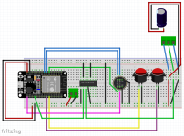
1708055276270.png

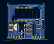
So I decided I'd move up to using something called KICAD. With KICAD, you draw up the schematic first, and then use a pcb design tool to layout the components and traces. I was surprised it wasn't all that hard to learn and was much easier to adjust footprints and trace widths.
This tutorial gave me all I needed to work through it. Kicad Tutorial
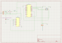
1708055516466.png1708055586526.png

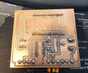
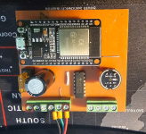
This is what I ended up. Not the greatest soldering job in the world , but the board works just fine.
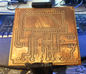
1708055767896.png1708055930605.png

1708055874583.png1708056019878.png


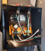
And this is the end result. Now I need to get the records out of the stack of boxes in the bedroom and onto the shelves!
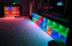
1708056210210.png
 
Last edited:
Nice!

So what kind of bit did you use for the milling? and what sizes are the drill holes?
The milling bit is a 1/8" 60 degree Vbit with a .1mm tip and I use a .5mm drill for the holes. I'll then use some hand drills to make the holes bigger to fit the components.
 
Last edited:
I've got another board I need to work on tomorrow, I'll go through some of the other details in the actual milling process in another post and document some of the other apps I use.
 
So, I'm not going to go into how to use KiCad or how to design a PCB using it, as that's a pretty long topic and there are much better resources for that out there. Suffice to say what you really want to get to is a point where you can export the gerber files from KiCad.

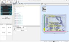
Once The gerbers are generated, I've found Carbide Copper to be a quick and easy way to generate Gcode.

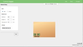
The first thing I do is to just setup the size of the blank board. 100mmx70mmX1.6mm
CC_1.JPG

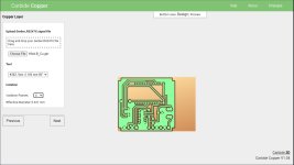
Since this is a single sided board, I import the import the bottom Copper layer.
Set the bit to a 60 degree .1mm bit. Since my soldering can be a little bit sloppy, I generate 4 isolation passes, which is how many times it goes around to isolate the traces from the rest of the board.
CC_2.JPG

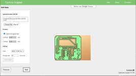
Next up set up the drill holes and import your .drl file. I set for a fairly slow plunge rate of 10mm/min. I've been using a .5mm drill bit. It fits the smaller holes I need. For the bigger holes, I go ahead and use a little pin vise and bits to enlarge the required holes.
CC_3.JPG

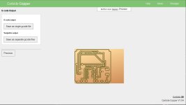
You can skip over the next few screens until you get to the g-code output. I save mine as seperate gcode files.
CC_4.JPG


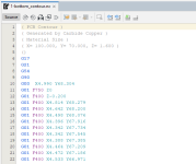
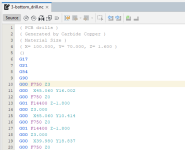
The one issue I have with the gcode is that after I upgraded my grbl version, it would go to x0y0z0 and then drag the spinning bit across the board until it would start to do the milling.
So I insert a "G00 F750 Z3" command to just scoot the z up 3mm to keep it out of the way. I do that to both the copper bottom and the drill files.
1708475047616.png1708474938456.png
 

Attachments

  • UGS Autolevel Setup 2.JPG
    UGS Autolevel Setup 2.JPG
    248.2 KB · Views: 1
  • UGS Probe Setup.JPG
    UGS Probe Setup.JPG
    242.8 KB · Views: 1
  • CC_FIX_2.JPG
    CC_FIX_2.JPG
    35.7 KB · Views: 1
  • CC_FIX_2.JPG
    CC_FIX_2.JPG
    35.7 KB · Views: 0
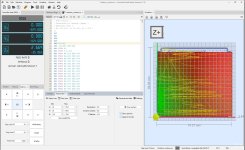
As far as sending the code to the machine, I'm using UGS "Universal Gcode Sender". It has the ability to probe an autolevel the pcb to make sure you get a nice even milling.
Blank PCB's are not necessarily all that flat and with the very shallow cuts we are taking, it's important to autolevel. This will allow the Z to move ever so slightly up and down when milling based on the readings.

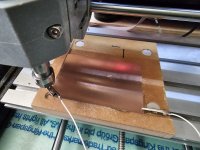
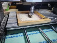
So, First up, I attached a little piece of MDF to the CMC build plate and used a 1/8 " bit to mill a section of the spoil board flat. I sprayed it with some clear poly to protect the spoil board and to give it a bit of a smoother finish to hold the pcb boards.
If you look at the picture, you can see I've got 2 wires connected to cnc to use for probing. I also dug a little divot on the far right side to hold the clip to the board. The other clip goes onto the bit.
20240219_164311.jpg

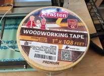
I use some of this 'WoodWorking Tape' double sided tape to hold the pcb blank to the spoil board. Not sure why it took me so long to find this, but it works so much better than the old carpet tape I used to use.
1708475411771.png

The first step is to probe the board for the z height. I use the probe tab in UGS. The important thing is to make sure you start your probe and autolevel probing from the same spot. I pick the very lower left of the board.
Make sure, and double make sure you have the alligator clips attached, click the Z in the little left window, then click 'Probe and Zero Z'.
UGS Probe Setup.JPG

Next up we want to probe the surface of the board. It took me a while to figure out the settings to get this to work correctly.
I set mine up for doing 5mm grids over the size of the pcb.
Click Scan Surface and let it run.
UGS Autolevel Setup 2.JPG

So Then We're ready to go. Carbide Copper doesn't insert the spindle start commands, so I manually turn on the spindle using "M03 S20000;".
I did upgrade the machine to have a 20k rpm spindle and also a balanced collet.
Click the start button and it will run the program.
I spritz the board with some Denatured Alcohol to use as a cutting fluid. It makes for much smoother cuts and keeps from lifting the copper at the edges.
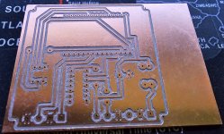
Once the trace cuts have been made, swap out the bit for the .5mm drill and go back to the same probe position and probe Z with the new bit.
Load the drill file, start up the spindle, and run the drill program.
20240219_173221.jpg
And here we go. This is ready now for enlarging the holes and then soldering.
I should say that what I'd like to do is to figure out how to apply a solder mask. My experiments on that so far have been messy and unsuccessful, but I do plan on work on it at some point.
20240220_160342.jpg
 
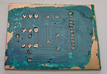
So, This is round one of trying to do a solder mask. Ugly, but functional. I'll bake a little more of it on those areas around the edges to make it look a 'little' better.

1708629219086.png

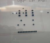
The basic process was that I exported the solder mask as an SVG file from kicad, pulled that into Inkscape, made the color of the spots 'black'. Then I printed it out on a transparency sheet. I actually ran it through the printer 2x to get the ink as black as possible. Let that dry for a few minutes.
1708629373929.png

I forgot to get a picture of the initial smearing of the solder mask paste. Basically, I taped the board to a scrap piece of ply, put a little paste on the board and smeared it around with an old hotel plastic room key. IT actually looked pretty good at that time.

I then lined up and stuck the transparency on the board, and used a little roller to smash that into the paste.

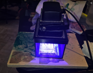
I then Used a little UV light to partially cure the solder mask. I went for 2 90 second blasts of uv light with a 90 second rest in between.

This is my UV curing setup. A little uv light on top of a 3d printed base.
1708629268233.png

Like I said, this is ugly, but it's mostly functional. I'll bake a little more on it then I'll solder it up.

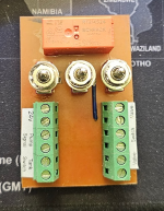
this is for adding some control functions to my irrigation storage tank on the hill. Basically adding some switches to be able to manually fill the tank and manually turn on the irrigation pump.

I have some other ideas on how to do this that will not be as messy or ugly, but need to wait for some tooling to arrive. Just thought I'd give this a shot.
 
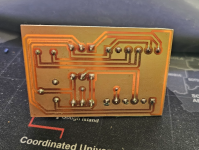
After a few iterations, I finalized my pump control panel. I kind of gave up on the solder resist mask for now.

The isolation cuts are thick enough I didn't really have any issues. I did protect the copper by giving it a couple of coats of clear flexseal, lol. That oughta work.
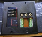
1710003143817.png1710003263344.png

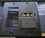
Printed up a custom outlet plate for it with a little access cover to get at the screw terminals. This goes on an outdoor outlet box out by the pump and tank so will be protected from the weather.
A 24v AC transformer gets plugged into a gfci outlet on the left.

1710003296357.png1710003582103.png


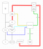
Basically, this will let me control the booster pump, the tank fill, and shut off valve to the irrigation system. I can set each of them to either work automatically, manually, or to OFF.
1710003849528.png
 
Top